The Role of Photoresist
Photoresist is a material that plays a vital role in microelectronics manufacturing, semiconductor processing and other high-precision patterning processing fields. The following is a detailed introduction to its specific role:
1. Pattern transfer role
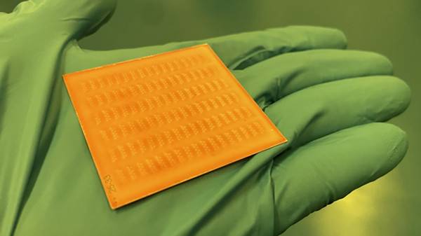
In precision processing such as semiconductor chip manufacturing, photoresist acts as a key medium for pattern transfer. Its basic principle is based on photolithography technology. The designed circuit pattern is transferred from the mask (a template with a pre-designed pattern) to the photoresist layer through photolithography equipment (such as a photolithography machine). The specific steps are as follows:
- Coating photoresist: First, the photoresist is evenly coated on the surface of the substrate material to be processed (such as a silicon wafer) to form a layer of photoresist film. The thickness of this film is usually between a few hundred nanometers and a few microns. The specific thickness depends on the subsequent processing requirements.
- Exposure process: Then, the substrate coated with photoresist is exposed through the mask using light of a specific wavelength (such as ultraviolet light) emitted by the photolithography equipment. In the exposed area, the photoresist will undergo corresponding chemical changes according to its own characteristics (such as positive photoresist or negative photoresist, the difference between the two will be described in detail later). For example, positive photoresist will become soluble in the developer in the exposed area, while negative photoresist will become more insoluble in the developer in the exposed area.
- Development operation: After the exposure is completed, the development operation is then carried out. The substrate coated with photoresist is placed in the developer. At this time, according to the chemical changes of the photoresist during exposure, the photoresist in the unexposed area (for positive photoresist) or the exposed area (for negative photoresist) will be dissolved and removed by the developer, leaving a pattern corresponding to the pattern on the mask on the photoresist layer, realizing the pattern transfer from the mask to the photoresist layer.
2. Protective substrate
The photoresist can also protect the substrate material during the processing process, preventing the substrate from unnecessary damage or contamination in subsequent processing steps such as etching and ion implantation. The specific performance is as follows:
- Etching protection: In the etching process, some unnecessary materials need to be removed from the substrate to form a specific circuit structure or other shape. For example, in the manufacture of semiconductor chips, it may be necessary to remove metal or semiconductor materials in certain areas of the silicon wafer by etching to form circuit connections, transistors and other structures. In this process, the photoresist coated on the substrate plays a protective role. The etching solution will only remove the areas not covered by the photoresist, while the areas covered by the photoresist are protected and will not be corroded by the etching solution, ensuring that the parts of the substrate that need to be retained are completely retained.
- Ion implantation protection: Ion implantation is another common semiconductor processing technology used to inject specific types and doses of ions into the substrate material to change the electrical properties of the substrate material. During the ion implantation process, photoresist also plays a protective role, preventing the injected ions from affecting the areas on the substrate where ion implantation is not required, ensuring that the ion implantation operation is only performed in the predetermined area, and protecting the original structure and performance of the substrate.
3. As a selective barrier for processing technology
The existence of photoresist enables selective processing in complex processing technology, that is, different operations are performed on the substrate material according to the coverage of the photoresist, which is mainly reflected in the following aspects:
- Chemical plating selectivity: In the chemical plating process, by controlling the coverage of the photoresist, selective chemical plating can be achieved on different areas of the substrate. For example, when manufacturing certain electronic components, a metal film needs to be plated on a specific area of the substrate. By first coating the substrate with photoresist, and then exposing and developing it according to the design pattern, only the area where the metal film needs to be plated is not covered by the photoresist. In this way, when chemical plating is performed, metal ions will only be deposited in the area not covered by the photoresist to form a metal film, realizing selective chemical plating.
- Photoresist’s selective barrier effect on different processing technologies: Photoresist not only plays a selective barrier role in the above-mentioned etching, ion implantation, chemical plating and other processes, but also plays a similar role in some other processing technologies such as diffusion and sintering. By reasonably setting the coverage of the photoresist, the action area of different processing technologies on the substrate material can be controlled, and refined processing operations can be achieved to improve processing accuracy and product quality.
4. Different action characteristics of positive photoresist and negative photoresist
Photoresist is mainly divided into positive photoresist and negative photoresist, which show different characteristics in the above-mentioned various effects:
- Positive photoresist:
– Pattern transfer characteristics: Positive photoresist becomes soluble in the developer in the exposed area, so after development, the photoresist in the exposed area is removed, leaving the photoresist in the unexposed area to form a pattern corresponding to the mask. This characteristic makes positive photoresist more advantageous in the manufacture of fine patterns, because finer patterns can be obtained by precisely controlling the exposure area, and it is often used in fields such as semiconductor chip manufacturing that require high pattern accuracy.
– Processing technology selectivity: In etching, ion implantation and other processing technologies, the unexposed areas of positive photoresist play a protective role. Because the photoresist in these areas is not removed, the corresponding areas on the substrate can be protected from the influence of these processes, which conforms to the general logic of processing technology, that is, protecting the unoperated areas. - Negative photoresist:
– Pattern transfer characteristics: Negative photoresist becomes more insoluble in the developer in the exposed area, so after development, the photoresist in the unexposed area is removed, leaving the photoresist in the exposed area to form a pattern corresponding to the mask. This characteristic makes negative photoresist more commonly used in the manufacture of some relatively simple products that do not require particularly high pattern accuracy, such as the manufacture of some printed circuit boards (PCBs).
– Processing technology selectivity: In etching, ion implantation and other processing technologies, the exposed areas of negative photoresist play a protective role. Because the photoresist in these areas is retained, the corresponding areas on the substrate can be protected from the influence of these processes. It is different from the protection method of positive photoresist, but it can also achieve the protection of the substrate and the selective operation of the processing technology.
In short, photoresist is an indispensable material in the fields of microelectronics manufacturing, semiconductor processing, etc. Through its multiple functions such as pattern transfer, substrate protection, and as a selective barrier, it helps to achieve high-precision and refined processing operations, laying an important foundation for the development of modern electronic technology.
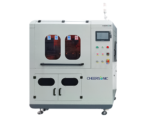
Ultrasonic spraying systems have been proven to be used in various applications that require uniform and repeatable photoresist or polyimide film coatings. The thickness control range is from submicron to more than 100 microns, and any shape or size can be coated.
Ultrasonic spraying technology is used for semiconductor photoresist coating. Compared with traditional coating processes such as spin coating and dip coating, it has the advantages of high uniformity, good encapsulation of microstructures, and controllable coating area. In the past 10 years, it has been fully demonstrated that the 3D microstructure surface photoresist coating using ultrasonic spraying technology, the prepared photoresist coating is significantly higher than the traditional spin coating in terms of microstructure wrapping and uniformity Craft.
The ultrasonic spraying system can precisely control the flow rate, coating speed and deposition volume. Low-speed spray shaping defines atomized spray as a precise and controllable pattern to avoid excessive spray when producing a very thin and uniform layer. The ultrasonic spray system can control the thickness from sub-micron to more than 100 microns, and can coat any shape or size.
About Cheersonic
Cheersonic is the leading developer and manufacturer of ultrasonic coating systems for applying precise, thin film coatings to protect, strengthen or smooth surfaces on parts and components for the microelectronics/electronics, alternative energy, medical and industrial markets, including specialized glass applications in construction and automotive.
Our coating solutions are environmentally-friendly, efficient and highly reliable, and enable dramatic reductions in overspray, savings in raw material, water and energy usage and provide improved process repeatability, transfer efficiency, high uniformity and reduced emissions.
Chinese Website: Cheersonic Provides Professional Coating Solutions


