
Ultrasonic Spray Coating Machine for Semiconductor Chips
Ultrasonic Spray Coating Machine for Semiconductor Chips
With the accelerated localization of the semiconductor industry and continuous breakthroughs in advanced processes, semiconductor chips, as the core foundation of the electronics industry, are widely used in diverse fields such as consumer electronics, industrial control, automotive electronics, communication equipment, and aerospace, encompassing various types including logic chips, memory chips, and power chips. Semiconductor chips use silicon, silicon carbide, and other substrates as substrates, and are manufactured through multiple precision processes such as photolithography, etching, and spray coating. Their integration, operational stability, and lifespan directly depend on the coating quality of the passivation layer, insulating layer, and conductive layer. Currently, semiconductor chips are developing towards smaller processes and higher integration, placing more stringent demands on the precision and cleanliness of the spray coating process. Cheersonic ultrasonic spray coating machines, with their core advantages of high precision, low damage, and high adaptability, perfectly meet the precision spray coating needs of semiconductor chips, breaking through the bottlenecks of traditional processes, providing core equipment support for the large-scale, high-quality mass production of chips, and contributing to the breakthrough of localization in the semiconductor industry.
The precision structure and advanced manufacturing processes of semiconductor chips impose far higher standards on coating processes than on ordinary devices, and their performance is deeply intertwined with coating quality. The core coating steps for chips include passivation layer coating, insulating protective layer coating, and metal electrode conductive layer coating. The coating thickness needs to be precisely controlled between 0.03-0.8μm. The core coating requirements focus on three main aspects: First, high uniformity coating, requiring precise control of coating thickness and distribution with a deviation ≤ ±0.01μm and uniformity exceeding 99%. Defects such as pinholes, bubbles, and particle agglomeration must be avoided to ensure a dense, gap-free coating, guaranteeing pure signal transmission, preventing short circuits and leakage, and adapting to the high-density circuitry requirements of advanced process chips. Second, low-damage adaptation, as semiconductor chip substrates are fragile and internal circuitry is intricate (linewidth can be…). The coating process, from nanometer-scale coatings to passivation layers and conductive pastes, is sensitive to high temperatures and pressures. The entire process requires low pressure and temperature control to prevent high-pressure impacts from damaging the chip structure and lattice integrity. Simultaneously, it must ensure strong adhesion between the coating and the chip surface, resisting subsequent high-temperature annealing and encapsulation processes without cracking or peeling. Thirdly, it demands high cleanliness and compatibility, meeting Class 100 or higher cleanroom standards to eliminate micro-dust contamination and avoid interfering with the chip’s electrical performance. It must also be compatible with different types of coating pastes, ensuring seamless coating of complex structures such as chip trenches and micro-electrode gaps, meeting the fabrication needs of various semiconductor chip types, including advanced processes and power chips.
Currently, in the semiconductor chip coating field, traditional coating processes (high-pressure gas atomization spraying, spin coating, sputtering) have many shortcomings, making them difficult to adapt to the demands of precision fabrication and large-scale mass production, thus becoming a bottleneck restricting the localization of semiconductor production. High-pressure gas atomization spraying easily introduces impurities and moisture, leading to chip contamination and performance degradation. High-pressure airflow can also damage delicate chip circuitry, and material utilization is only 25%-35%, failing to meet the low-defect requirements of advanced process chips. Spin coating has a material utilization rate of less than 30%, wasting large amounts of expensive coating materials. High-speed rotation can generate stress, causing lattice defects in the chip and affecting its lifespan. Sputtering equipment is costly and the process is complex; high-energy particle bombardment can easily damage the chip structure, and it is difficult to adapt to coating complex structures such as trenches and micro-gap areas without dead angles, resulting in poor adaptability and difficulty meeting the needs of large-scale mass production.
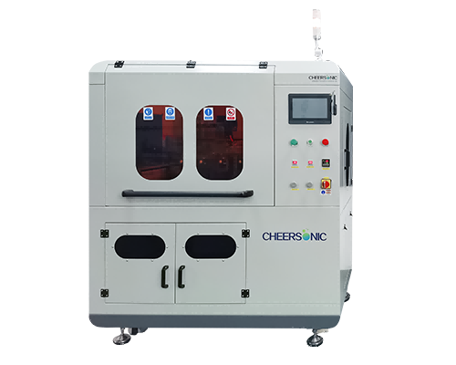
Cheersonic ultrasonic spraying machines, targeting the characteristics and spraying pain points of semiconductor chips, rely on high-frequency ultrasonic atomization core technology and combine it with key points of semiconductor chip manufacturing processes to create customized solutions, completely breaking through the bottlenecks of traditional processes and helping to solve the problem of domestic production of high-end coatings. The equipment converts industrial frequency electricity into a 40-150kHz high-frequency electrical signal via an ultrasonic generator. This signal is then converted into high-frequency mechanical vibration by a piezoelectric ceramic transducer. Utilizing the ultrasonic cavitation effect, passivation and conductive slurries are atomized into fine droplets of 0.01-2 microns, effectively deagglomerating particle clusters in the slurry and precisely controlling the solvent evaporation rate. This ensures a uniform, fine, dense, and void-free coating, perfectly meeting the core requirements of high integration and low defects in semiconductor chips, thus helping to improve the electrical performance and reliability of the chips. The atomization process is conducted under low pressure and temperature control, with no impurities introduced. The droplets are gently deposited on the chip surface and in the gaps by a slight carrier gas, without mechanical contact or high-pressure impact, thus preventing damage to the chip structure and delicate circuitry. The spraying parameters can be flexibly adjusted to adapt to different processes and types of semiconductor chips, and it is compatible with automated large-scale production lines, meeting the mass production needs of the semiconductor industry.
For the coating needs of semiconductor chips, Cheersonic ultrasonic spraying machines exhibit four core advantages, helping companies achieve large-scale, high-quality chip mass production. First, ultra-precise and uniform coating achieves a coating uniformity of over 99% and a thickness deviation of ≤±1%, effectively ensuring stable chip signal transmission, preventing defects, and meeting the stringent requirements of advanced process chips.
Second, low-damage protection utilizes low-pressure, gentle atomization technology to avoid damage to the chip substrate and delicate circuitry, balancing coating adhesion and chip integrity, improving product yield, and helping to reduce chip manufacturing costs.
Third, high material utilization, reaching over 95%, significantly reduces waste of expensive spray coating slurry, meeting the economic needs of large-scale semiconductor production.
Fourth, excellent mass production adaptability supports automated continuous spraying and compatibility with Class 100 cleanrooms, seamlessly integrating into large-scale semiconductor chip production lines, adapting to complex structures with no dead angles, solving the problems of low efficiency, high loss, and poor consistency of traditional processes, and facilitating the transformation of chips from laboratory-grade to engineering applications.
Currently, Cheersonic ultrasonic spray coating machines are widely used in various semiconductor chip spraying scenarios, covering core products such as logic chips, memory chips, and power chips. They are compatible with core fields such as consumer electronics, automotive electronics, and communication equipment, helping companies solve problems such as chip damage, low yield, and material waste caused by traditional spraying processes, providing strong support for the mass production of domestically produced semiconductor chips. As a leading enterprise in the field of ultrasonic electronic equipment, Cheersonic Ultrasonic has been deeply involved in the semiconductor chip spraying field for many years, closely following the trend of chip development towards advanced processes and high integration. Drawing on advanced coating technology experience in the industry, it can provide customized spraying solutions, covering the entire process from equipment selection and process parameter optimization to slurry adaptation. In the future, Cheersonic Ultrasonic will continue to optimize equipment performance, further improve atomization accuracy and process adaptability, help the semiconductor industry break through technological monopolies, and inject strong momentum into the high-quality development of semiconductor localization and advanced packaging.

About Cheersonic
Cheersonic is the leading developer and manufacturer of ultrasonic coating systems for applying precise, thin film coatings to protect, strengthen or smooth surfaces on parts and components for the microelectronics/electronics, alternative energy, medical and industrial markets, including specialized glass applications in construction and automotive.
Our coating solutions are environmentally-friendly, efficient and highly reliable, and enable dramatic reductions in overspray, savings in raw material, water and energy usage and provide improved process repeatability, transfer efficiency, high uniformity and reduced emissions.
If you have any technical questions, customization demands, or procurement inquiries about ultrasonic atomization nozzles, feel free to contact our professional sales and technical team for detailed parameters, customized solutions, and industry application support.
Email: market2@cheersonic.com