
spraying positive electron beam photoresist
spraying positive electron beam photoresist – Cheersonic
In high-end fields such as micro-nano fabrication, advanced semiconductor packaging, and precision device manufacturing, electron beam resist, as a core consumable in electron beam lithography, directly determines the accuracy of pattern transfer and device performance. Positive electron beam resist, as a high-performance electron beam resist, has become the preferred product for mid-to-high-end electron beam lithography scenarios due to its excellent resolution, good etching resistance, and process adaptability. Positive electron beam photoresist is a type of polymer photosensitive resin consumable, specifically designed for electron beam lithography. It achieves pattern curing through a polymer cross-linking reaction triggered by electron beam irradiation. It boasts key advantages such as high resolution, low shrinkage, and strong adhesion. A single coating can achieve a film thickness of 0.5-50μm, with a maximum resolution below 100nm. After development, the pattern edges are clean, with no residue or swelling. It exhibits excellent compatibility with commonly used electron beam developers and is suitable for various substrates including silicon wafers, glass, and metals. It is widely used in micro/nano structure fabrication, semiconductor packaging, precision sensor manufacturing, and photomask processing. Uniform coating of electron beam photoresist is crucial for ensuring the precision of electron beam lithography. Cheersonic ultrasonic spraying machines, with their high precision, low damage, and high compatibility, perfectly meet the spraying requirements of positive electron beam photoresist, providing core equipment support for improving the quality and efficiency of high-end photolithography processes.
The characteristics of positive electron beam photoresist and the requirements of the entire electron beam lithography process place extremely stringent standards on the coating equipment. Electron beam lithography achieves precise fabrication of micro- and nano-patterns by focusing an electron beam onto positive electron beam photoresist. The core reliance is on the uniformity and cleanliness of the photoresist layer. The key coating requirements are concentrated in three main aspects: First, extremely uniform coating. This requires precise control of the positive electron beam photoresist film thickness, adapting to a coating range of 0.5-50μm with a deviation ≤±0.05μm and a uniformity of over 98%. Defects such as pinholes, bubbles, and particle agglomerations must be avoided—these defects can lead to uneven photosensitive exposure during electron beam irradiation, blurred pattern edges, and burrs, affecting the dimensional accuracy of the micro- and nano-structures. Simultaneously, the surface of the photoresist film must be smooth to meet the precise requirements of focused electron beam irradiation, providing a smooth surface for subsequent etching processes. First, it provides a stable foundation; second, it offers low-damage and high-cleanliness. The polymer structure of positive electron beam photoresist is sensitive to impact and high temperature. The spraying process must be gentle and without impact or high temperature to avoid damaging the molecular structure of the photoresist layer and its adhesion to the substrate, preventing cracking and peeling of the photoresist layer during exposure and development. At the same time, it meets the clean production standards of semiconductors, eliminating the introduction of impurities and particles, avoiding affecting the accuracy of electron beam lithography, and ensuring device performance; third, it is flexible and adaptable, enabling adaptation to different sized substrates and various electron beam lithography scenarios, precisely controlling the spraying range, eliminating waste of positive electron beam photoresist, balancing spraying efficiency and process consistency, adapting to the high-speed scanning characteristics of electron beam lithography, and helping to improve the mass production efficiency of micro and nano devices.
Traditional positive electron beam photoresist spraying processes (spin coating, air spraying, manual coating) have many shortcomings and are difficult to adapt to their characteristics and the needs of large-scale mass production. While spin coating can achieve a certain degree of uniformity, it is only suitable for flat substrates, and the material utilization rate is less than 40%, resulting in the waste of a large amount of expensive positive electron beam photoresist. High-speed rotation can easily aggravate the stress of the photoresist layer, leading to cracking during subsequent electron beam exposure. It cannot meet the coating requirements of non-flat substrates and complex micro-nano structures, and it is difficult to meet the high-resolution photolithography requirements below 100nm. Air spraying relies on high-pressure airflow atomization, resulting in uneven droplet size, which can easily produce pinholes and bubbles. High-pressure impact can damage the polymer structure of positive electron beam photoresist, and high-pressure airflow can easily introduce impurities, affecting the cleanliness of the photoresist film. The nozzle is prone to residue and blockage, resulting in high maintenance costs. It cannot meet the high-precision requirements of high-end electron beam lithography. Manual coating is inefficient, with poor coating uniformity and consistency, and is prone to uneven thickness and irregular edges. Human operation can easily cause substrate contamination. It is only suitable for small-batch research and development in the laboratory and cannot meet the large-scale mass production requirements in fields such as semiconductors and precision sensors.
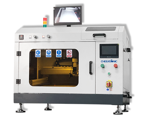
Cheersonic ultrasonic spray coating machine addresses the characteristics and process challenges of positive electron beam lithography. Utilizing core high-frequency atomization technology, it has undergone specialized optimization and incorporates key aspects of the entire electron beam lithography process to create a customized solution, completely breaking through traditional process bottlenecks. The equipment converts industrial frequency electricity into a 40-150kHz high-frequency electrical signal via an ultrasonic generator. This signal is then converted into high-frequency mechanical vibration by a piezoelectric ceramic transducer. The ultrasonic cavitation effect deagglomerates particle clusters in the positive electron beam lithography, preventing defects such as pinholes and particles caused by agglomerates. Stable atomization is achieved without excessive dilution, forming fine droplets of 0.01-3 micrometers with high particle uniformity, perfectly suited to coating requirements of 0.5-50μm and high-resolution lithography requirements below 100nm. Guided by a low-pressure carrier gas, droplets gently deposit onto the substrate surface without high-pressure impact or high-temperature generation. This process maximizes the preservation of the high resolution and high etching resistance of positive electron beam photoresist, reduces internal stress in the photoresist layer, avoids pinholes and orange peel problems caused by excessive solvent evaporation, and prevents the introduction of impurities. It also enhances the adhesion between the photoresist layer and the substrate, forming a dense, uniform, and smooth high-quality photoresist layer, laying a solid foundation for subsequent electron beam irradiation, exposure, development, and etching processes.
For the spraying needs of positive electron beam photoresist, Cheersonic ultrasonic spraying machine demonstrates four core advantages, helping enterprises to improve mass production quality and efficiency. First, it offers extremely high coating precision, accurately controlling the thickness and distribution of the resist layer with a deviation of ≤±1% and uniformity exceeding 98%, ensuring the precision of micro-nano patterns below 100nm, avoiding coating defects, and improving electron beam lithography yield. Second, it features low-damage compatibility, with low-pressure gentle atomization technology avoiding damage to the molecular structure and substrate of the positive electron beam photoresist, reducing resist layer stress, and avoiding problems such as cracking and peeling, meeting clean production requirements, and adapting to coating non-planar substrates and complex micro-nano structures. Third, it boasts high material utilization, reaching over 95%, significantly reducing positive electron beam photoresist waste and saving substantial consumable costs compared to traditional spin coating processes, aligning with the concept of green and low-carbon production. Fourth, it offers excellent mass production adaptability, supporting automated continuous spraying and cleanroom compatibility, seamlessly integrating into large-scale semiconductor and micro-nano device production lines, adapting to different thicknesses and types of positive electron beam photoresist and various substrates, solving the problems of low efficiency, high loss, and poor consistency in traditional processes.
Currently, Cheersonic ultrasonic spray coating machines are widely used in the spraying of positive electron beam photoresist, covering core areas such as micro/nano structure fabrication, semiconductor packaging, precision sensor manufacturing, and photomask processing. This helps companies solve the pain points of traditional spray coating processes, achieving improved quality of positive electron beam photoresist coating and efficient implementation of electron beam lithography. As a leading company in the field of ultrasonic electronic equipment, Cheersonic Ultrasonic has been deeply involved in the high-end photolithography spraying field for many years, keeping abreast of the development trend of electron beam lithography technology. It can provide customized spraying solutions, covering the entire process from equipment selection and process parameter optimization to positive electron beam photoresist adaptation, helping customers fully leverage the core advantages of this electron beam photoresist. In the future, Cheersonic Ultrasonic will continue to optimize equipment performance to meet the needs of electron beam lithography’s upgrade towards greater precision and efficiency, injecting strong momentum into the high-quality development of micro/nano processing and the semiconductor industry.

About Cheersonic
Cheersonic is the leading developer and manufacturer of ultrasonic coating systems for applying precise, thin film coatings to protect, strengthen or smooth surfaces on parts and components for the microelectronics/electronics, alternative energy, medical and industrial markets, including specialized glass applications in construction and automotive.
Our coating solutions are environmentally-friendly, efficient and highly reliable, and enable dramatic reductions in overspray, savings in raw material, water and energy usage and provide improved process repeatability, transfer efficiency, high uniformity and reduced emissions.
If you have any technical questions, customization demands, or procurement inquiries about ultrasonic atomization nozzles, feel free to contact our professional sales and technical team for detailed parameters, customized solutions, and industry application support.
Email: market2@cheersonic.com