
Flip Chip Principles & Advantages, Semiconductor Advanced Packaging Guide
Inside smartphones, high-speed communication devices and various sensors, a chip is far more than a simple silicon die. Apart from wafer fabrication processes, advanced packaging also determines signal transmission speed, heat dissipation capability and integration density of chips. Flip Chip is one of the core technologies widely adopted in this field.
Traditional chip packaging uses wire bonding. The chip faces upward, and fine metal wires connect chip pads to the substrate. These metal wires are limited in length, creating longer signal transmission paths that cause loss and interference for high-frequency signals. Besides, it is difficult to expand the number of pins on a large scale. Flip Chip changes this approach: the chip is flipped, with the pad-bearing side facing downward to directly bond with the packaging substrate via solder bumps. Replacing thin metal wires, solder bumps greatly shorten signal routes to deliver higher transmission bandwidth. More I/O pins can be arranged on the chip surface to meet the demand for high-density interconnection.
The workflow of Flip Chip follows a clear logic. First, tiny solder bumps are fabricated on chip pads. Then alignment equipment precisely flips the chip to match solder bumps one-to-one with corresponding pads on the substrate. Metallurgical bonding is completed through reflow soldering. After interconnection, a narrow gap remains between the chip and substrate. Underfill is injected into this gap, acting as a protective barrier for the Flip Chip structure. It relieves thermal stress between the chip and substrate caused by different thermal expansion coefficients, preventing solder bump cracking under temperature cycling and mechanical vibration and improving long-term device reliability.
The coating process of underfill directly affects packaging yield. Ultrasonic spraying is adopted in the industry to atomize the underfill material and deposit it evenly around gaps. Compared with traditional dispensing, it delivers thinner and more consistent coatings, fitting high-density, narrow-gap Flip Chip packaging scenarios. This non-contact coating method exerts no mechanical impact on micro solder bumps, suitable for delicate advanced packaging processes.
Flip Chip boasts prominent advantages. For one thing, the short signal path reduces parasitic inductance and resistance for excellent high-frequency performance, ideal for high-speed computing and radio frequency communication. Secondly, pin density rises significantly, allowing more interconnection channels within a limited area. Thirdly, heat dissipation gets improved, as the active side of the chip sits close to the substrate to conduct heat outward faster and ease overheating of high-power chips.
Nevertheless, this technology comes with high process barriers. Ultra-high requirements are imposed on substrate flatness and alignment accuracy; micron-level offset will lead to cold solder joints. Stress mismatch from different thermal expansion coefficients must be mitigated through optimized underfill materials and processes. Equipment and material costs are higher than conventional wire bonding packaging. Initially applied only to high-end chips, it has gradually spread to mid-to-high-end devices as processes mature.
Flip Chip technology keeps evolving and spawning more branches of advanced packaging, laying the foundation for heterogeneous integration. Chips with diverse functions can be interconnected by Flip Chip and assembled in one package. There is no need for all chips to adopt the most advanced manufacturing nodes. Instead, packaging realizes computing integration to cut R&D costs effectively. From computing chips in data centers and automotive electronics to miniature sensors, Flip Chip supports electronic products toward smaller size, faster speed and stronger performance.
Wafer fabrication engraves circuits on silicon wafers, while advanced packaging reliably connects individual chips. As a key packaging technology, Flip Chip, paired with fine manufacturing processes such as ultrasonic spraying, continuously pushes the performance limit of microelectronic devices and remains an indispensable part of the semiconductor industry.
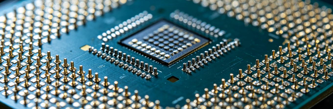
Flip Chip Technology
Flip Chip Technology Flip Chip serves as the core [...]
To reach our anytime via email please fill out the form below with your request and a company representative will reply to you. To find your local CHEERSONIC representative to connect directly click your region in the contact drop down menu.

Contact CHEERSONIC For immediate assistance please contact us the corporate headquarters during business hours at 6:00 am – 22:00 pm.
Tel: 0571-87910406
- Mobile: +86 15869049660
- Email: Market2@cheersonic.com
Add: 11-13 Chuangye Road, Changkou, Fuyang, Hangzhou, Zhejiang, China
