
Microelectronics: The ‘Coating Magic’ Hidden in Chips
When you pick up your phone, put on a smartwatch, or start a new energy vehicle, you cannot do without the support of microelectronics technology. Microelectronics is the discipline of researching and manufacturing micro – or even nano scale electronic devices, ranging from a small chip to a large display screen, all of which belong to its territory.
In microelectronics manufacturing, there is a seemingly insignificant but crucial process – thin film coating. Whether it is the photoresist on the chip, the conductive layer in the display screen, or the protective film on the sensor surface, a uniform and ultra-thin functional thin film needs to be plated on the substrate. Traditional methods such as spin coating, although common, have problems such as large material waste and difficulty in covering complex surfaces.
At this point, ultrasonic spraying technology made its debut. It uses high-frequency vibration to atomize liquid into micrometer sized droplets, and then sprays them accurately onto the target surface at low speed. This “non-contact” process has several advantages: firstly, it has a high material utilization rate, which can significantly reduce the waste of expensive chemicals such as photoresist; Secondly, the coating has good uniformity, which can maintain consistent thickness even on complex morphologies with through holes and traces; Thirdly, it has strong compatibility with solvents and is suitable for various formulations.
In the field of advanced packaging, ultrasonic spraying can evenly coat photoresist on large-sized panels, supporting semiconductor manufacturing of larger specifications. In MicroLED displays, it can spray extremely thin flux on millions of micro solder pads, remove oxide layers, improve soldering yield, and directly affect the reliability of the display screen. In the deposition of nanomaterials such as carbon nanotubes and nanowires, ultrasonic vibration can naturally disperse aggregated nanoparticles, allowing them to recover their independent state and maintain optimal electrical and optical properties.
In addition, ultrasonic spraying is widely used in EMI electromagnetic shielding, MEMS sensor functional layers, flip chip soldering, and other scenarios. From laboratory research and development to mass production lines, it can smoothly transition and become an indispensable “coating wizard” in microelectronics manufacturing.
As chips become smaller and devices become more precise, the requirements for thin film coatings will also become increasingly high. Ultrasonic spraying technology is providing a solid guarantee for the continuous advancement of the microelectronics industry with its precise, efficient, and environmentally friendly characteristics.
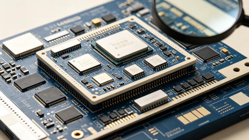
Photoresist for Panel-Level Packaging | Key Material for Advanced Packaging Lithography
Photoresist for Panel-Level Packaging Photoresist for Panel-Level Packaging | Key [...]
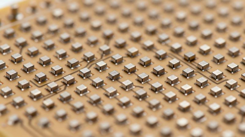
Microelectronics Coating Knowledge
Microelectronics Coating KnowledgeGain a deep understanding of precision thin [...]
